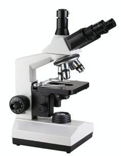
Microscope imaging principle
An electron microscope is an instrument that replaces the light beam and optical lens with electron beams and electron lenses according to the principle of electron optics, so that the fine structure of the substance can be imaged at a very high magnification.
The resolving power of an electron microscope is expressed by the minimum distance between two adjacent points it can resolve. In the 1970s, the resolution of the transmission electron microscope was about 0.3 nanometers (the resolution of the human eye was about 0.1 millimeters). The maximum magnification of the electron microscope is now more than 3 million times, while the maximum magnification of the optical microscope is about 2000 times, so through the electron microscope, you can directly observe the atoms of some heavy metals and the neatly arranged atomic lattice in the crystal.
In 1931, Knorr and Ruska, Germany, modified a high-voltage oscilloscope with a cold cathode discharge electron source and three electron lenses, and obtained images magnified more than ten times, which confirmed the possibility of magnified imaging with an electron microscope. . In 1932, after Ruska's improvement, the resolution of the electron microscope reached 50 nanometers, which was about ten times the resolution of the optical microscope at that time, so the electron microscope began to attract people's attention.
In the 1940s, Hill in the United States used an astigmatism to compensate for the rotational asymmetry of the electronic lens, which made the resolution of the electron microscope a new breakthrough and gradually reached the modern level. In China, the transmission electron microscope was successfully developed in 1958, with a resolution of 3 nanometers. In 1979, a large electron microscope with a resolution of 0.3 nanometers was made.
Although the resolution ability of the electron microscope is far better than that of the optical microscope, the electron microscope needs to work under vacuum conditions, so it is difficult to observe living organisms, and the irradiation of the electron beam will also cause biological samples to be damaged by irradiation. Other issues, such as the brightness of the electron gun and the improvement of the quality of the electronic lens, also need to be further studied.
The resolving power is an important index of electron microscopy, which is related to the incident cone angle and wavelength of the electron beam passing through the sample. The wavelength of visible light is about 300 to 700 nanometers, and the wavelength of the electron beam is related to the acceleration voltage. When the acceleration voltage is 50-100 kV, the wavelength of the electron beam is about 0.0053-0.0037 nm. Since the wavelength of the electron beam is much smaller than the wavelength of visible light, even if the cone angle of the electron beam is only 1% of that of the optical microscope, the resolving power of the electron microscope is still far superior to that of the optical microscope.
The electron microscope is composed of three parts: lens barrel, vacuum system and power cabinet. The lens barrel is mainly composed of electron gun, electronic lens, sample holder, fluorescent screen and photographic mechanism. These parts are usually assembled into a cylinder from top to bottom; the vacuum system is composed of mechanical vacuum pump, diffusion pump and vacuum valve, etc. The gas pipeline is connected with the lens barrel; the power cabinet is composed of a high-voltage generator, an excitation current stabilizer and various adjustment control units.
The electron lens is the most important part of the electron microscope tube. It uses a space electric field or magnetic field symmetrical to the axis of the lens tube to bend the electron trajectory toward the axis to form a focus. Its function is similar to that of the glass convex lens to focus the beam, so it is called electron. lens. Most modern electron microscopes use electromagnetic lenses. The strong magnetic field generated by a very stable DC excitation current through the coil with pole shoes causes the electrons to focus.
The electron gun is a component composed of tungsten hot cathode, grid and cathode. It can emit and form an electron beam with a uniform speed, so the stability of the acceleration voltage is required to be no less than 1 in 10,000.
Electron microscopes can be divided into transmission electron microscopes, scanning electron microscopes, reflection electron microscopes and emission electron microscopes according to their structures and uses. Transmission electron microscopes are often used to observe the structure of fine materials that cannot be distinguished by ordinary microscopes; scanning electron microscopes are mainly used to observe the morphology of solid surfaces, and can also be combined with X-ray diffractometers or electron spectrometers to form electrons. Microprobe is used for material composition analysis; emission electron microscope is used for self-emission electron surface research.
The projection electron microscope is named after the electron beam penetrates the sample and then uses an electronic lens to magnify the image. Its optical path is similar to an optical microscope. In this electron microscope, the contrast of image details is formed by the scattering of electron beams by the atoms of the sample. The thinner or lower-density part of the sample has less electron beam scattering, so that more electrons pass through the objective diaphragm and participate in imaging, which appears brighter in the image. Conversely, the thicker or denser parts of the sample appear darker in the image. If the sample is too thick or too dense, the contrast of the image will deteriorate, and it may even be damaged or destroyed by absorbing the energy of the electron beam.
At the top of the transmission electron microscope barrel is an electron gun. The electrons are emitted from the tungsten hot cathode and pass through the first and second condenser lenses to focus the electron beam. After passing through the sample, the electron beam is imaged on the intermediate mirror by the objective lens, and then enlarged step by step through the intermediate mirror and the projection lens, and imaged on the fluorescent screen or photographic dry plate.
The intermediate mirror mainly adjusts the excitation current, and the magnification can be continuously changed from tens of times to hundreds of thousands of times; by changing the focal length of the intermediate mirror, electron micrographs and electron diffraction images can be obtained on the tiny parts of the same sample . In order to be able to study thicker metal slice samples, the Dulos Electron Optics Laboratory in France has developed an ultra-high voltage electron microscope with an acceleration voltage of 3500 kV. Scanning electron microscope structure diagram
The electron beam of the scanning electron microscope does not pass through the sample, and only secondary electrons are excited by scanning on the surface of the sample. The scintillation crystal placed next to the sample receives these secondary electrons and, after amplification, modulate the electron beam intensity of the kinescope, thereby changing the brightness on the kinescope fluorescent screen. The deflection coil of the kinescope keeps synchronous scanning with the electron beam on the surface of the sample, so that the fluorescent screen of the kinescope displays the topography image of the surface of the sample, which is similar to the working principle of industrial television.
The resolution of the scanning electron microscope mainly depends on the diameter of the electron beam on the sample surface. The magnification is the ratio of the scanning amplitude on the kinescope to the scanning amplitude on the sample, which can be continuously changed from tens of times to hundreds of thousands of times. Scanning electron microscopes do not require very thin samples; the images have a strong three-dimensional effect; they can use information such as secondary electrons generated by the interaction of electron beams and substances, absorbed electrons, and X-rays to analyze the composition of substances.
The electron gun and condenser of the scanning electron microscope are roughly the same as those of the transmission electron microscope, but in order to make the electron beam thinner, an objective lens and an astigmatism are added under the condenser, and two sets of mutually perpendicular scans are installed inside the objective Coil. A sample stage can be moved, rotated and tilted in the sample chamber under the objective lens
Liyang Paper Products Co., Ltd. was established in 1999,a professional enterprise integrated in R&D,Marketing and Manufacturing.Liyang Printing provide best solutions and service to various fields of industry.For example,we can make nice and luxury Notebook .Such as PU Notebook ,Spiral Notebook,Custom Notebook,School Notebook,Leather Notebook,softcover notebook,hardcover notebook,etc.Our notebook with high quality are exquisite printing for your products.
We are committed to offering packaging solutions to help customers improve sales volume.
Any inquiries on our notebook,welcome to contact us at any time.


Notebook
Notebook With Pen,Spiral Notebook,Custom Notebook,School Notebook,Notebook,Paper Notebook,PU Notebook
Liyang Paper Products Co., Ltd. , https://www.liyangprinting.com